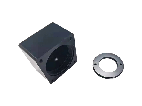
Semiconductor electronic parts processingin addition to the well-known "design, manufacturing, packaging, testing" four links, the middle of the overall link is actually very complex, can be divided into the front section of the process and after the process.
Semiconductor electronic parts processing begins with the most basic material - silicon wafer, by making circuits and electronic components (such as transistors, capacitors, logic gates, etc.) on silicon wafer, for the above processes require the most complex technology and the most capital investment process.
Because the chip is a high-precision product, so the manufacturing environment has high requirements, its required manufacturing environment is a temperature, humidity and dust all need to control the dust-free room.
Here are the main production processes:
Silicon wafer materials
A wafer is a silicon wafer used to make a silicon semiconductor IC. The material is silicon, the silicon wafer used by chip manufacturers is silicon crystal, because the whole silicon wafer is a single and complete crystal, so it is also called single crystal.
But in the whole solid crystal, the direction of many small crystals is not phase, it is a complex crystal (or polycrystal). The formation of single crystals or polycrystals depends on the temperature, rate of crystal growth and impurities.
Two, optical development

Optical development is the process of exposure and development on the photoresist to convert the image on the mask to the film layer or silicon crystal below the photoresist.
Optical development mainly includes photoresist coating, baking, mask alignment, exposure and development procedures. The resolution of small size image, but also in the progress of IC process, plays a key role. Due to the need of optics, yellow visible light is used for illumination in this process. So commonly known as this area yellow light area.
Three, etching technology
Etching is the removal of material by chemical reaction and physical impact. Can be divided into: wet etching: wet etching is the use of chemical solution, after chemical reaction to achieve the purpose of etching; Dry etching: Dry etching uses a type of plasma etching.
The role of etching in plasma etching may be the physical effect of plasma ions impacting the surface of the chip, or the chemical reaction between plasma free radicals and surface atoms of the chip, or even the combination of the above two. The main application now is plasma etching technology.
CVD chemical vapor deposition
Chemical vapor deposition refers to the reaction of chemical gases or vapors on the substrate surface to synthesize coating or nanomaterials. It is the most widely used technology in the semiconductor industry to deposit a variety of materials, including a wide range of insulating materials, most metal materials and metal alloys.
About us
Company profileCulture EnvironmentDetectionContact usProduct Center
Medical parts processingLaser parts processing Semiconductor parts processingLithium battery accessories processing Electronic parts processing view moreApplication field
Medical device industryLaser equipment industrySemiconductor industryRobot spare parts applicationMarine spare parts industryNews center
company dynamicIndustry dynamicFAQScan the QR code
 Website QR code
 Wechat QR Code