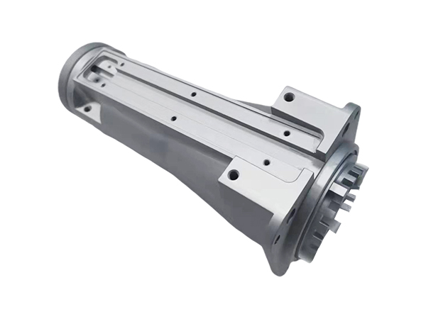
Semiconductor electronic parts processingconsists of the following steps and is repeated:
lithography
etching
Thin film (chemical or physical vapor deposition)
Doping (thermal diffusion or ion implantation)
Chemical mechanical flattening CMP
Monocrystalline silicon wafers (or III-V family, such as gallium arsenide) are used as the base, and then MOSFET or BJT components are made using photolithography, doping, CMP, etc., and wires are made using thin film and CMP technology. Due to product performance requirements and cost considerations, wires can be divided into aluminum process (mainly spatter plating) and copper process (mainly electroplating see Damascene).

The main technology can be divided into the following categories: yellow light microfilm, etching, diffusion, film, flattening, metallization.
Semiconductor electronic parts are the most common type of integrated circuit, so the highest density device is memory, but even microprocessors have memory.
Despite their complexity, chips have been shrinking in width for decades, but the layers of integrated circuits are still much thinner than their width.
The component layers are made very much like a photographic process. Although the light waves in the visible spectrum cannot be used to expose the component layers, they are too large.
High-frequency photons (usually ultraviolet) are used to create patterns for each layer. Because each feature is so small, an electron microscope is a necessary tool for a process engineer tuning a manufacturing process.
About us
Company profileCulture EnvironmentDetectionContact usProduct Center
Medical parts processingLaser parts processing Semiconductor parts processingLithium battery accessories processing Electronic parts processing view moreApplication field
Medical device industryLaser equipment industrySemiconductor industryRobot spare parts applicationMarine spare parts industryNews center
company dynamicIndustry dynamicFAQScan the QR code
 Website QR code
 Wechat QR Code